It’s Time to Stop Kicking the EDA Dog
, 2015年06月16日
As SoC designers, we are usually insulated from the back-end of the chip design process. We don’t encounter the place and route and timing closure problems that must be resolved by others to turn our front-end logic designs into real chips. Those problems often create challenges that delay our project schedules and prevent us from bringing our chip to market in a timely fashion. To reverse these delays, the industry needs to do a better job of improving the front-end design so it can avoid problems in the back end.We often develop a floorplan for our SoC design and throw our RTL and net list files over the wall to the back-end integrators who must turn it into real placed gates and macros. Our designs may seem logical, conceptually, but when problems arise in the back end, the common practice is to blame the inadequacy of EDA tools and their users.
As an IP vendor, I say it’s time to stop kicking the EDA dog.
It’s incumbent on IP vendors to deliver higher quality designs that enable a smoother back-end process, and avoid the problems that cause chips to be late to market.
Front-end and back-end teams sometimes work for different companies, but even those within the same company often don’t work closely together. IP vendors need to be aware of all the struggles that back-end teams encounter when trying to close timing on complex designs.

Physical challenges of SoC design can originate at the start of the project, progress to the early NoC, floorplan stages and produce ramifications in the final stages.
It is obvious to most chip architects that certain IPs should be physically close to each other. This is particularly true for CPUs and memory controllers. But problems for the back-end teams often arise with the less standard elements of SoCs, such as DSPs, image accelerators, dedicated security encryption engines, peripheral devices, camera and display controllers and the like.
When it comes time to place such IP blocks, problems with the floorplan create problems in the top-level interconnect, and it’s up to back end team to fix the problems that originate with the front-end team. For complex designs, this can take numerous iterations over a period of many months.

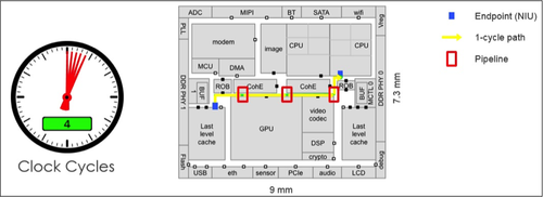
Because of growing complexity, signals can’t cross in one cycle even best-in-class 28nm processes. Back-end times have to insert pipeline stages to achieve timing closure, a process that can last for weeks and months.
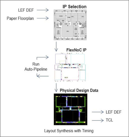
Interconnect fabric IP needs to be aware of the physical constraints of the back-end layout. Network-on-chip IP also needs to be physically aware. In addition to highlighting issues before they become physical placement and timing problems, the IP should be able to automatically provide an architecture with appropriate pipelining that completely avoids the common timing closure difficulties that back-end teams usually encounter.
This article was originally published in EE Times.
