Streamlining Interconnect Integration Accelerates Globally Distributed Design
, 2015年03月03日

The problem arises because chipmakers split up design tasks so each team works to the strengths of its expertise. One team will design the basic architecture at headquarters and then parcel out the graphics portion to Design Team A. Design Team B gets to work on the processor complex and Design Team C is set to optimize video and audio processing. But the connectivity portion of the chip has to work with all the other subsystems. When each individual team completes its work in meeting performance goals and design constraints, then a designated interconnect team has the task bringing all this work back together into the final SoC.
Parceling Out Creates Bottlenecks
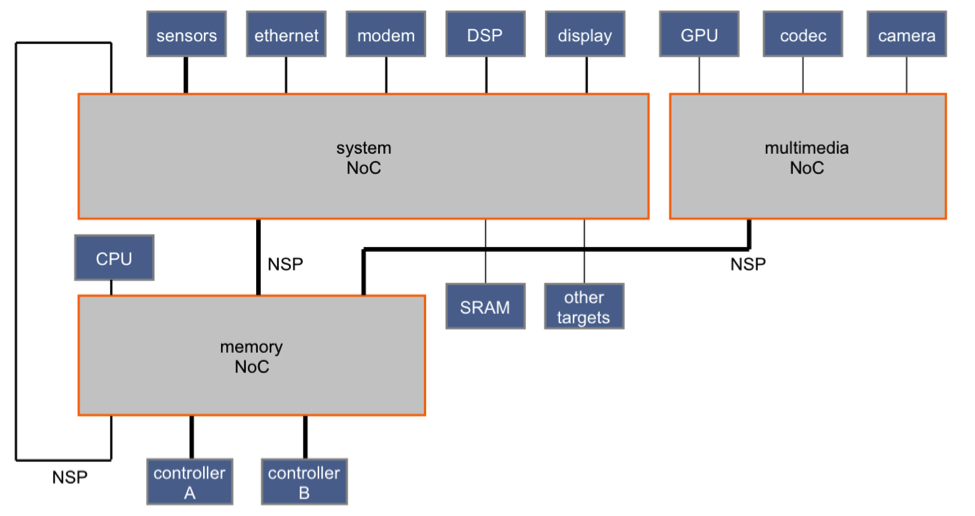
Complexity grows as more and more IP designs are integrated. As each IP evolves into its own subsystem, it becomes increasingly difficult to parcel out the tasks to the distributed design centers. The centers might be located in different locations around the world or they might work in the same building as HQ. Regardless, each has created its own interconnect within the subsystem they are assigned to work on. Now, all of those subsystems have to work with the top-level interconnect fabric to ensure that they are operating in conjunction with all of the other different subsystems.
The main problem pops up when it comes time to bring all the work back together. Different parts of the chip may not communicate properly with each other because as each team makes changes to their subsystem interconnect, other teams are also changing theirs. Integration requires the ability to synchronize these changes.
As each one of the separate interconnects becomes more complex within its own subsystem, it takes more time to stitch all the other subsystems together. And all of this has to be verified at the block or subsystem level, and then re-verified at the top SoC level. These extra steps delay schedules and push out time to market.
SoCs that use a hybrid bus or crossbar architecture as the interconnect fabric are particularly prone to this misadventure. When it comes time to bring all the blocks together to operate as a single SoC, it requires some shim logic to make all the connections work harmoniously. Many global design teams have accepted this additional work as part of the process even though it takes time and makes final verification more difficult.
Implement a Single Platform Strategy
Teams are striving to find a better way to integrate all of the distributed design efforts. The successful ones utilize a single platform strategy. Each group of engineers gets to work on their particular area of expertise and, once their work is completed, all of the different interconnects within all of the different subsystems can now be stitched together seamlessly into one network-on-chip interconnect fabric. All the connections operate correctly and verification is straightforward and successful. This interconnect consolidation can now take place in a matter of minutes or days instead of weeks and months. Market-specific SoCs can now be produced in as little as 7 to 8 months instead of 24 to 36 months.
With a single platform strategy, chipmakers typically produce one top-of-the-line SoC, and then turn that basic design into derivatives to address vertical markets. If the first SoC is an application processor for high-end smart phones, then that same architecture can be handed off to the company’s design teams with expertise in the tablet or automotive market. That team can strip away some of the functional blocks needed for mobility and integrate the IP specifically suited for target market applications. This process is now occurring more rapidly than ever before.
Streamlining the Distributed Design Process
Chip companies that accelerate the distributed design process can integrate all of the individual interconnects from all the SoCs subsystem into one. This enables design teams to cut development time from 18 months to as little as nine months. These teams can take the same SoC and parcel out the tasks to each of its design teams around the world. For example, Team A can optimize the platform for tablet applications, Team B can reconfigure the SoC for the feature phone market, and Team C can build a derivative for home entertainment systems.
Parceling the SoC architecture enables different design “centers of excellence” to work simultaneously — around the world if need be — on its separate piece. The game changer is the ability to easily integrate all the separate subsystem interconnects into one top-level interconnect fabric once all of the individual teams have completed their design work. The process allows all the interconnections between the separate blocks to come together seamlessly, no matter how IP block addressing, transaction protocols, or command sets change during the development process. This also makes final verification process for the chip much easier and faster. The end result is a shorter development time, shorter time to market, and more potential revenue and profit.
This article was originally published in Semiconductor Engineering magazine.
